

Use of Scanning Electron Microscopy for Material Characterisation
- Dec 30, 2024
- 2 min read
Scanning Electron Microscopy (SEM) and Energy Dispersive X-Ray Spectroscopy (EDS) have an important place in the work of ticemlabs with their material characterisation capability and observation capacity up to nano-dimensions.
SEM-EDS can provide the necessary data for materials research, quality control, contaminant identification and damage analysis by performing surface visualisation and targeted elemental analysis. For this reason, it is used in building material analysis and architectural restoration projects within our laboratories.
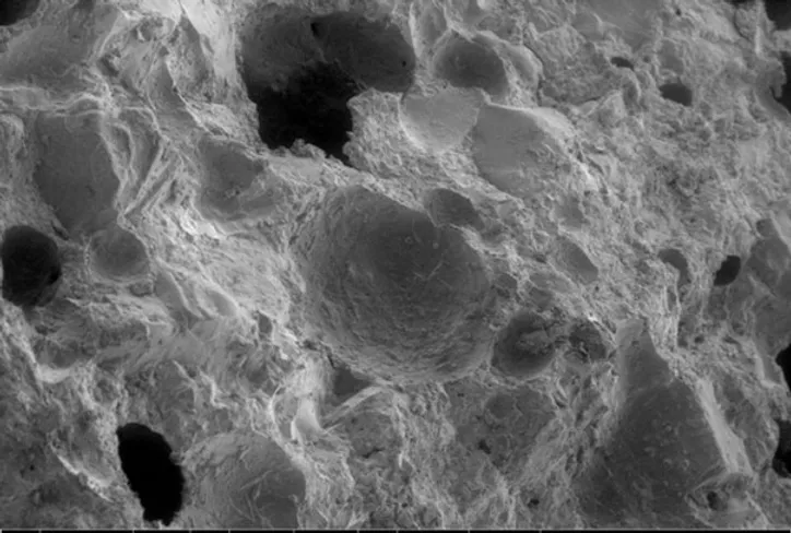
The samples placed in the SEM are imaged with Back Scattered Electrons (BSE) and Secondary Electron (SE) systems accelerated in the voltage range of 4.8 to 15 kV. Thanks to the electron images created, surface forms that reveal the material properties of a sample such as mineral formations, surface roughness, surface cracks can be examined. The SEM in our laboratories also offers Automatic Image Mapping application. In this application, multiple SEM images are automatically collected and combined to obtain a single image for larger areas.
Situations where the size and number of specimens must be kept to a minimum are frequently encountered in the architectural restoration sector and in high-cost product design processes. In such cases, SEM-EDS, which analyses in micro volumes, is one of the most efficient techniques. In this system where samples of 100 x 32 mm and smaller can be analysed, the samples must be conductive or coated with conductive materials such as gold and carbon. Powder products can be examined by surface fixation.
SEM images are supported by Energy Dispersive X-Ray Spectroscopy (EDS) for advanced information about the material. EDS technique determines the chemical composition of the sample by revealing the distribution of elements on the sample surface. By determining a point or line on the sample, detailed elemental analysis can be performed and graphical data can be provided. Thus, the presence and change of elements in a point or direction and the percentage data of the elements in the composition can be found. In addition, it is also possible to produce colour coded elemental maps with the area scan option. The distribution of elements in the sample can be observed with detailed maps produced according to the desired resolution and measurement timing. Point analyses and elemental maps can be used together to provide the highest level of information for an area.
Ticemlabs has conducted SEM-EDS analyses for textile reinforced mortars, cement based products, metal-epoxy structural adhesive systems, repair mortars and historical building materials.


Comments